PLANAR OPTICS DESIGN MADE SIMPLE
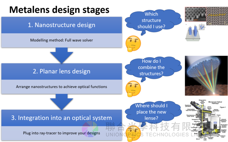
PlanOpSim software unites the different stages of designing metasurface and planar optics components in one tool. The same software calculates and models the three key steps in metalens design:
· Nanostructure modelling: a powerful solver calculates the behaviour of nanoscale elements also called meta-atoms in detail from Maxwell's equations
· Component design: holographic optimization algorithms arrange the nanostructures to produce the optical functions you specify
· System integration: the results of PlanOpSim calculations can be directly plugged into widely used ray-tracers to calculate the metasurface's performance in the final application
PlanOpSim runs on any standard desk- or laptop. No cluster setups or supercomputers are needed.
Nanostructure Design
Designing nanostructures and meta-atoms
PlanOpSim allows straightforward and fast simulation of the nanostructured building blocks of meta-surfaces. Any design of a meta-lens or other planar optics component starts with the design of the meta-atoms.
The nanostructures are modeled by a full wave solution of Maxwell’s equations. The unit-cell of a structure is surrounded by periodic boundaries.
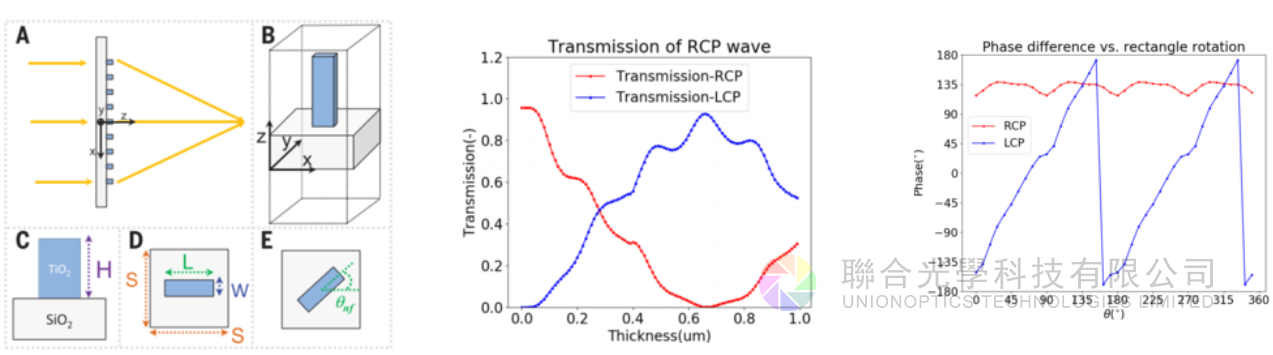
Example: TiO nano-fin elements
A popular class of meta-atoms are rectangular columns of high index material. The rectangular shape allows to control phase of circularly polarized light by the rotation of the fins in the substrate plane. The distance between structures is below a single wavelength to suppress diffraction. The strucure in this example was proposed in the paper by Khorasaninejad et.al. (DOI 10.1126/science.aaf6644). It consists of titanium dioxide nanofins on a soda-lime glass substrate.
PlanOpSim uses the rigourous coupled wave analysis method to rigoursly and rapidly simulate the response of a nano-fin. The structure used is shown in the figure on the left. The first optimization step is to tune the height of the TiO structure to act as a half wave plate, converting the incident right handed circular polarized light to left handed circular polarization. For the simulation wavelength the maximum polarization conversion is found for a thickness of 650nm.
We then use this thickness to model the relative phase differences for the different rectangle rotations. The plot on the right illustrates the Pancharatnam Berry relation that the relative phase retardation is twice the in-plane angle of the structure. So a series of rectangles with rotations between 0-180 degrees provides full control over the phase of the transmitted light over the entire 0-360 degree range. Khorasaninejad and colleaguess then go on to construct a meta-lens using these structures.
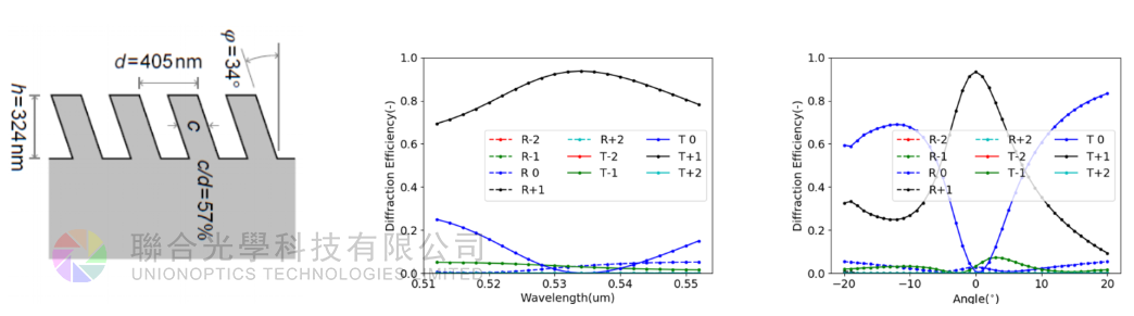
Example: simulating a diffraction grating
Diffraction gratings are often used as in- or outcoupling structures between light travelling in freespace and a waveguide structure. Slanted gratings like the one in on the left below are attractive because they can provide almost 100% diffraction efficiency into the 1st diffraction order. With PlanOpSim’s full wave solverthe diffraction can be accurately and quickly modelled. The center and right pictures show the changes in diffraction efficiency with the spectrum and angle of incidence of the incoming beam.
Slanted and blazed gratings are an interesting structure for coupling light into waveguides for head mounted displays for instance in virtual and augmented reality (VR & AR) headsets. The calculations above were executed within 5 minutes on a standard laptop.
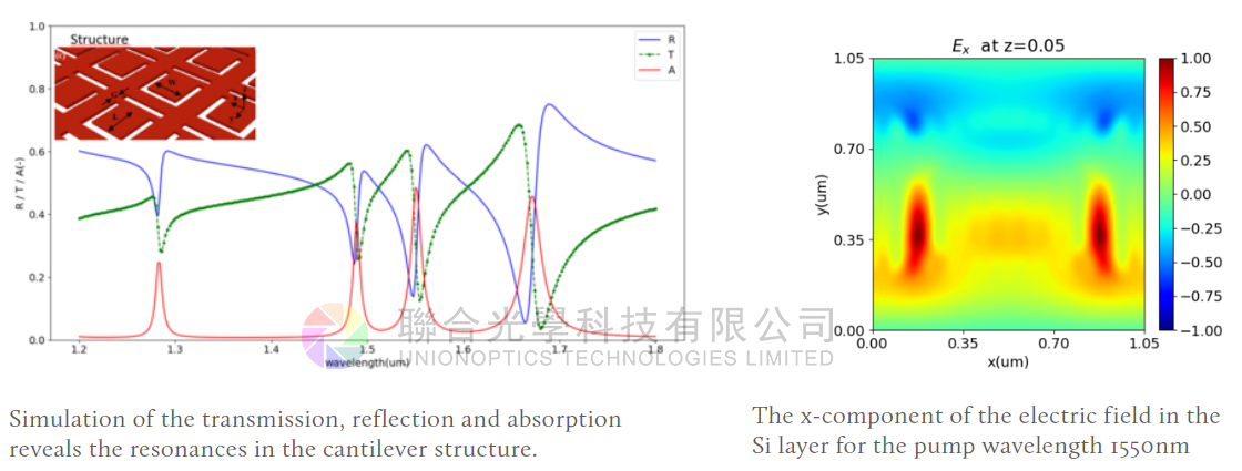
Example: analyse electric field profile inside an optomechanical cantilever
PlanOpSim can be used to simulate the profile of electric fields inside a complicated nanostructure. You can easily analyze the profile of the components of the electric and magnetic field. These profiles allow you too find the regions of strong electric field in the nanostructure where the light-matter interaction is the strongest.
In the example below the reflection and transmission of the Si cantilever structure in the insert is simulated. Karvounis et. al. used this structure to engineer a strong optomechanical response from a flaoting Si layer. By pumping the structure with a modulated beam at 1550nm the cantilever structure can be made to tilt up to 10 degrees. This can be sensed by a probe beam at 1310nm. The forces acting on the cantilever can be calculated from the electric field components.
You can find the full paper here:
1. Karvounis, A., Ou, J. Y., Wu, W., Macdonald, K. F. & Zheludev, N. I. Nano-optomechanical nonlinear dielectric metamaterials. Appl. Phys. Lett. 107, (2015).
Component Design
Component design for metasurfaces
With the right arrangement of nano-structures the metasurface can produce any optical reponse. With PlanOpSim software metasurfaces are defined easily and their response calculated. The software collects the full-wave results for each meta-atom. The behaviour of an entire surfac is then calculated using physical optics models. Components can be made both in a forward design where the structures are direclty choosen and placed or by inverse design where the target behaviour of the component is entered and the software determines the metasurface which produces that behaviour. Through combination of meta-atom design and placement, metasurfaces deliver characteristics that are impossible with conventional materials. Any classical optical component can be reproduced on a planar substrate as a metasurface as well.
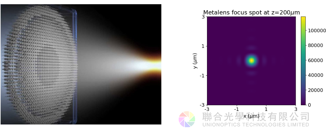
Metalens Example
Metalenses focus light through the co-operation of millions of sub-wavelength structures which individually manipulate the incident light locally. When the nano-structures are arranged to form a spherical wavefront a ‘perfect‘ (i.e. diffraction limited) lens is made. By traditional full wave modeling even a small 0.5x0.5 mm metalens is barely possible. With PlanOpSims combination of full wave and physical optics this task can be accomplished in a matter of minutes.
Above is an example of a metalens and its simulated intensity in the focal plane. The intensity profile shows the metalens produces a diffraction limited focus. The meta-atoms were simulated as Silicon Nitride pillars with diameter of 340nm and below on a glass substrate.
Inverse design: optimizing the projection of a holographic image
In real applications the intensity, polarization and spectrum you need, usually isn’t one where a textbook formula for the corresponding wavefront is easily found. PlanOpSim allows you to enter the target behaviour, the optimizer will then iterate through designs until the component matches the target behaviour.
Let’s say you want a diffractive optical element that projects the image of a cat when illuminated by a laser pointer. The optimization algorithm only needs to know the location and intensity of the image to calculate a nanostructure arrangement. Starting from a random first guess, the animation below shows how each trial solution approximates he target behaviour.
Integrated nano-structure calculation
PlanOpSims component level calculation is directly integrated with the full wave solutions of the nano-structures that make up the metasurface. When a meta-atom that was not known yet is discovered the model uses the full wave Maxwell equation solver to determine its response. The result is a powerful and versatile program to design metasurfaces. The method is fast enough to scan the design paramaters space in multiple directions. Tens of metalenses can be calculated in a matter of minutes.
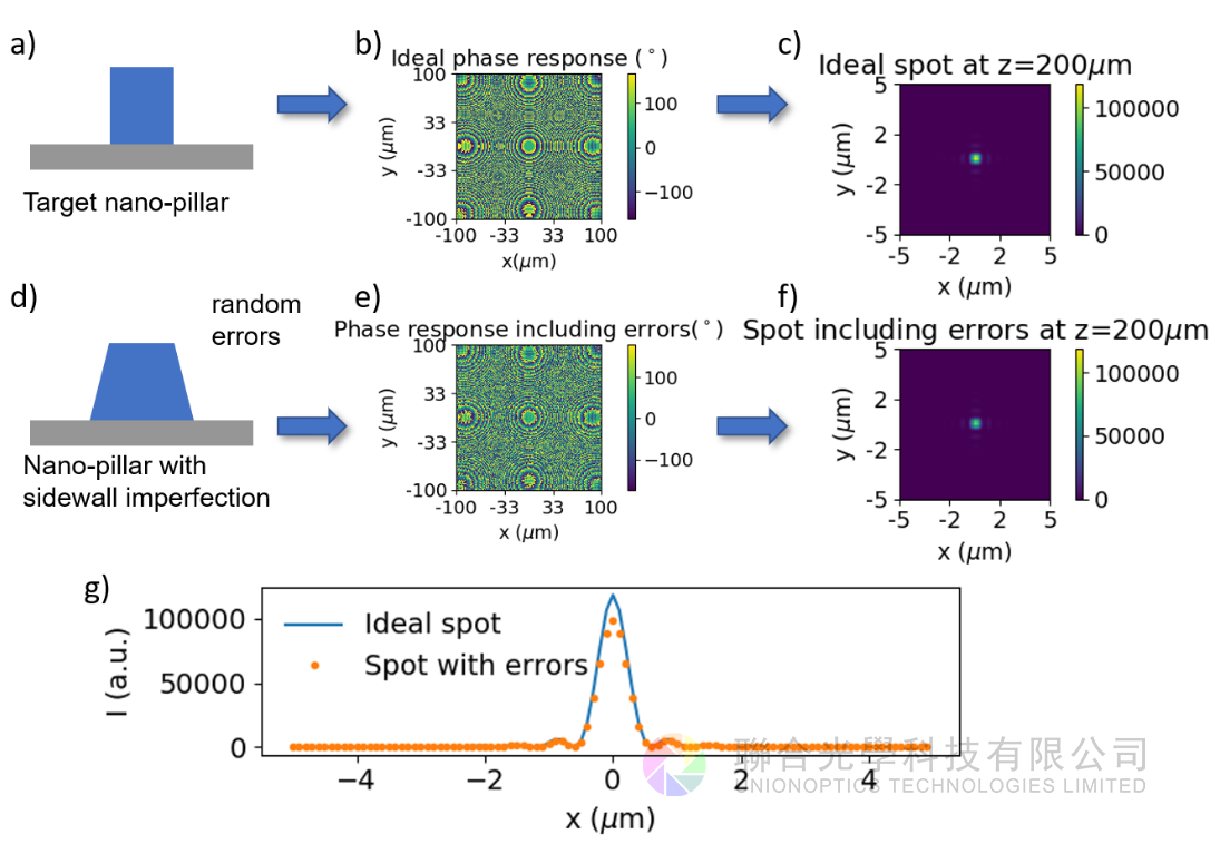
Thanks to high speed computation and the integrated full wave solver, PlanOpSim software was able to perform sensitiviy analysis on a metalens where each of the meta-atoms underwent random deformations. Taking the average of multiple lenses reveals critical knowledge for the fabrication of metalenses.
Monte carlo simulation of a metalens. Individual meta-atoms are randomized and their response calulated by the full wave solver. PlanOpSim component level simulation then computes the focal spot.